DIY PREAMPLIFIER DESIGN
DIY PREAMPLIFIER DESIGN
The Audio Designer nowadays must have two Laboratories - one equipped with adequate amounts of Test Equipment (dependant on the area of design) and the other, more importantly, equipped with the highest "Sonic Quality" pieces of Audio Equipment (for some this may even include competing brands). An Amplifier Designer must have an impeccable Turntable/Tonearm with a variety of Cartridges. Friends and Customers are an invaluable source of criticism in differing environments. The Loudspeakers used must be able to differentiate tone, soundstaging (ie. phase and times aligned), fine detailing without a particular sound of their own.
The CP3 was originally conceived as a means of "hearing" the sonic signature of its constituent components and to determine their exact effect on the sound quality of the unit. It also allowed me to hear the differences between transistor devices used in the same position before being incorporated into the more sophisticated topologies of my commercial designs. Identical transistors from different Manufacturers were found to possess distinct and different sonic colourations when substituted into the CP3 (In fact, when evaluating samples from batches of Semi-conductors for use in my commercial designs, this is one of my selection processes) inferences about Manufacture/Transistor quality could be made.
The CP3 's purity of sound can be traced to its simplicity. There are only three (3) semiconductors in the signal path from the phono input to the output - this includes the direct accommodation of a Moving Coil Cartridge without the extra Head Amp normally required. The RIAA Equalisation is entirely passive which does not affect the stability of the linear gain stages. The design formula included allows considerable variation to suit available component values. The ability to vary the quiescent operating current and loading enable considerable sonic optimisation with non-specified parts as well as the specified parts. The Regulated Power Supply ensures supply stability, and ripple/noise free operation. Using "REAL TIME" circuits eliminates the undesirable effects of negative feedback. The low parts count enables inexpensive construction and experimentation. The design is ongoing and and hence my own personal variations or improvements can be obtained by direct correspondence or by later details being published.
DIFFERENTIAL AMPLIFIER STAGES
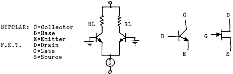
By using a differential gain stage, we ae not only simplifying the biasing requirements of the stage, but because of the symmertrical nature of the circuit, we are also significantly reducing the dominant second harmonic distortion figure. This is most effective when both devices are matched (see matching procedure) although even with severe mismathcing, this figure is still lower than with the equivalent single device stage. The only drawback is an increased noise figure.
The most significant factors influencing the "Sound Quality" are the BIASING CURRENT and DEVICE LOADING which also influence the GAIN/DISTORTION performance. The use of a "CONSTANT CURRENT" source regulating the BIASING CURRENT simplifies the design and allows considerable variations in gain, or device type used (F.E.T OR BIPOLAR).
I have elected to use both BIPOLAR (input stage) and F.E.T. (consecutive stages) in this design. If we compare the F.E.T to the BIPOLAR device in the same topology (Table 1) we will find that the BIPOLAR generaly has lower noise, higher gain (hence linearity) but does not possess the intrinsic high input impedance of the F.E.T and hence requires some form of input (BASE) biasing, ie., current into the BASE region.
There are three common methods of biasing the BASE region:
1. An impedance
matching network (buffer and capacitor);
2. A voltage divider network with input capacitor;
3. A low impedance source.
Typical Phono cartridges have a characteristic impedance of approximately 60 Ohms (High Output MM types) to as little as 1.0 Ohms (Low Output MC types). These inherent low impedance characteristics negate the need for the abovementioned networks, although the stage will not function correctly unless a Cartridge is connected (or a shunt resistor of equivalent value).
The less severe requirement of noise/gain, plus the high input impedance make the F.E.T the ideal device for the following stages of gain. If a High Output Cartridge was to be exclusively used, a F.E.T. input stage could be easily substituted for the BIPOLAR.
The gain of the individual Stages is dependant on:-
1. The BIASING
CURRENT "I" (Resistor which determines I as "RI");
2. The LOAD RESISTOR "RL";
3. The EMITTER DEGENERATION RESISTOR "RE".
The BIASING CURRENT (I) and the LOAD RESISTOR (RL) set up the quiescent conditions and maximum gain (when RE=O). The gain is reduced and linearity increased with the addition of RE (local feedback). To ensure utmost linearity we must maintain approximately 25VDC across the RL (when the voltage across RL is greater than 25V, a form of SLEW LIMITING will result). SInce the GAIN BANDWIDTH PRODUCT of a device is fixed, increasing the gain will lead to a decrease in bandwidth. An equation that relates RL to RI is:
PASSIVE RIAA EQUALISATION
There has currently been a trend towards the passive generation of the RIAA time constants with statements being made about its superiority over other forms of equalisation. I feel that although it can lead to excellent results sonically, it is only one of the design variables.
Its benefits are largely a result of its simplicity and lack of possible instability when used with separate amplification stages. It also possesses certain drawbacks. It requires relatively large values of capacitances which require high idling currents to overcome potential slew problems, and are harder to find with close tolerances or high quality that are typical of lower values, its noise performance is inferior and conflicting with input overload requirements, and finally it requires two stages of gain to allow for the losses generated.
Because of the high inherent impedance of the second gain stage (F.E.T), the capacitor values in the network can be reduced to values which can be found in tight tolerances and are easily trimmable.
PHONO TRIM STAGE
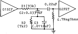
TRIMMING PROCEDURE
There are different elements reacting to determine the characteristics of the RIAA equalisation curve. These must be trimmed in a sequence.
1. DC Performance:
The 0.22uF capacitor resonating with the 4.74MegOhms
resistor -
fT = 1/2 x 3.14 x R x C = 0.1538 Hz (-3dB low frequ. pt)
2. 318uS turnover:
install the 82kOhms (R1), the 0.033uF capacitor (C2)
the 7kOhms (R2), as well as the 0.22/4.7MegOhms from (1) and trim R2 until
the gain between 500Hz and 1.0kHz is +2.65dB.
3. 75uF turnover: Now add C3 (0.0112uF) to the network and add or remove capacitance until the response at 20kHz relative to 1.0kHz is -19.62dB.
4. 3180uS turnover: R1 must now be trimmed to yield the correct gain at 20Hz relative to 1.0kHz (or at 50Hz rel. to 1.0kHz: +16.95dB) being +19.27dB. (This value is affected by the input stage load impedance, ie., RL1, and if RL1 is changed in value, R1 must be retrimmed).
These procedures require a high stability fixed amplitude SIne Wave Generator, a Frequency Counter and a "dB" Meter (FLUKE 8050A) (The SOUND TECHNOLOGY 1700B is a good Generator).
PHONO STAGE INPUT CAPACITOR REQUIREMENT
As mentioned earlier , since the impedance of the Phono Cartridge is low (less than 600 Ohms) it "biases" the Transistor input stage "on". This is due to the low impedance pathway created for the BASE CURRENT (Ib) to flow to GND through the Cartridge.
For those who are worried about "BASE CURRENT" flowing through the direct coupled Cartridge:
Ib = I/Hfe where I = BIASING CURRENT and Hfe = 400 for the LM394CH
= 2mA/400 = 5uA (the equivalent F.E.T. would have approximately
0.5uA "gate leakage).
This figure is insignificant and negates the need for an input Capacitor. A Capacitor in this section of the circuit is extremely undersirable since it would have to be a large value (more than 100uF) to satisfy the noise and low frequency performance. Typical large capacitors would significantly deteriorate the sonic performance.
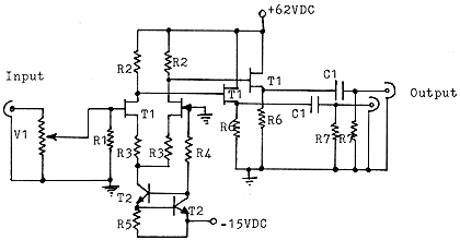
OUTPUT STAGE DESIGN
The Differential F.E.T. input used in the OUTPUT STAGE allows correct phase to be generated (normally a single gain stage would invert the phase by 180 degrees) as well as allowing a high input impedance necessary to accommodate all desirable inputs. VOLUME POTENTIOMETER values from 10kOhms to 100kOhms (logarithmic taper) can be used although the low frequency performance is determined by the preceding output capacitor, hence it is desirable that the higher values (100kOhms) be employed.
An interesting option with the differential stage is that the two outputs - inverting and non-inverting phase can be built into the design for comparison of its affect on the music.
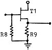
BUFFER
The unity gain F.E.T. Buffer offers the artifice of high input impedance and low output impedance. This improves the high frequency response and isolates the Gain Stages from the following Stages.
The simplicity of this Buffer can be exploited in an ACTIVE CROSSOVER that can be added as an option to this design at a later date.
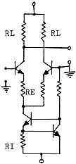
PHONO STAGE DESIGN
The resulting configuration that I have outlined here has emanated from a distillation of the variations that I have carried out to the prototype CP3 unit. This stage has been specifiçally designed for Moving Coil Cartridges, although for high output types, the input stage Emitter Resistors (RE1) should be increased to 100 Ohms.
Configuration 1.
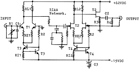
TABLE 2. PHONO STAGE (Bipolar input, F.E.T. consecutive Stage)
Phono Stage characteristics shown after varying RL, RE and RI. RL1, RE1 and RI1 refer to input stage. RL2, RE2 and RI2 refer to second stage.
| COND.** | RL1=10k RL2=16k | RL1=16k = RL2 | RL1=5.6k, RL2=16k |
| RE1 | 33 | 10 | 130 | 33 | 10 | 130 | 130 | 130 | 10 | 10 | 10 | 130 | 33 |
| RE2 | 130 | 130 | 130 | 390 | 390 | 130 | 680 | 390 | 390 | 130 | 130 | 130 | 130 |
| GAIN @1kHz |
46.3 | 52.5 | 36.3 | 41.5 | 48.0 | 40.0 | 31.5 | 35.0 | 48.5 | 53.0 | 51.5 | 33.5 | 44.0 |
| NOISE* | 63.0 | 70.0 | 53.5 | 62.0 | 68.0 | 57.0 | 53.0 | 55.0 | 69.0 | 70.5 | 68.5 | 50.0 | 61.0 |
T.H.D.1%***
| @20Hz | 1.4 | 0.7 | 5.0 | 4.0 | 2.4 | 3.6 | 22.0 | 10.5 | 3.2 | 0.7 | 1.0 | 12.0 | 3.6 |
| @1kHz | 28.0 | 15.0 | 85.0 | 60.0 | 28.0 | 62.0 | 215. | 125. | 30.0 | 14.0 | 15.0 | 125. | 36.0 |
| @20kHz | 185. | 77.0 | 630. | 180. | 75.0 | 320. | 320. | 320. | 120. | 58.0 | 115. | 1.1V | 300. |
** refers to RL, RI quiescent conditions.
| RL1=5.6kOhms | RI1=56Ohms |
| " =10kOhms | " =100Ohms |
| " = 16kOhms | " =200Ohms |
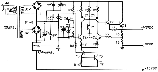
POWER SUPPLY
The Power Supply design featured in this article is a completely discrete, high speed, high transconductance, no compromise design which tightly regulates the voltage to the gain stages under STATIC and DYNAMIC conditions.
The most important element in this supply is the "SENSING ELEMENT" which on one side (BASE) features a fixed VOLTAGE REFERENCE and on the other derives its negative feedback to sense the ripple and harmonics on the DC supply line and by virtue of its feedback, eliminate the AC components from the pure DC that it regulates. A F.E.T. sensing device could be substituted for the BIPOLAR SENSING ELEMENT although would reduce the regulation effectiveness.
The SENSING ELEMENT is "actively loaded" to increase the gain and improve the PSRR (Power Supply Rejection Ratio) ie., decouple it from the influence of the unregulated PRIMARY FILTERING. The third device with its COLLECTOR to GND improves the "offset" characteristics of the SENSING ELEMENT.
The SERIES PASS ELEMENT (Output Stage) of the Supply is a NPN discrete Darlington configuration which has high input impedance (so that it does not load down or decrease the gain of the SENSING ELEMENT) and is selected to pass the necessary current to the gain stages. A high speed device is utilised which requires a degree of Heatsinking.
If stability problems are encountered, a small value (1.0uF) ELECTROLYTIC should be added across the output of the Supply to GND.
A separate -15VDC I.C. Regulator is employed to supply power to the "biasing" CONSTANT CURRENT sources which regulate the standing current of the GAIN STAGES.
SEMICONDUCTOR MATCHING PR0CEDURE
The process o matching devices offered for the CP3 is "in circuit" matching. This method of matching is more accurate than the usual methods of Hfe, Gfs, or using a Curve Tracer. It is preferable that the Emitter Resistor (RE) is shorted for this procedure as it will show a superficially better match when present.
The BASES or GATES of the devices to be matched must be connected to GND and a VOLTMETER be used to measure the voltage across RL. When the devices are matched, the voltages across both RL's should be equal.
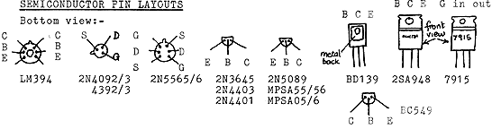
SEMICONDUCTOR FIN LAYOUTS
Bottom view:-
CONSTRUCTION
The recommended construction of this unit is on a high quality PC Board. Ground Plane boards will eliminate any stray hum and RFI interference pickup, although VERO or DIRECT WIRING techniques may also be applied.
The unit may be partially assembled as Phono Stage or with the addition of simple switching schemes, may be used as a fully fledged Control Preamplifier. (See CP details).
Because of the nature of the circuit, an extra stage of gain is not required even when using the lowest output Transducers.
CAPACITORS: The highest quality "Film" type capacitors should be used between stages and especially in the RIAA Network. This selection should be based on the "sonic signature" of the different dielectrics that are available.
WIRE: Apart from the PC tracks, pure SILVER or COPPER LITZEN should be used in this area, and should be kept as short as possible.
PRIMARY FILTERING: The Transformers and primary rectification/filter Capacitors should be housed in a separate enclosure with a 1.0 metre umbilical DC arrangement. The Regulation must be present near the Gain Stages to improve the HF, harmonic filtering action.
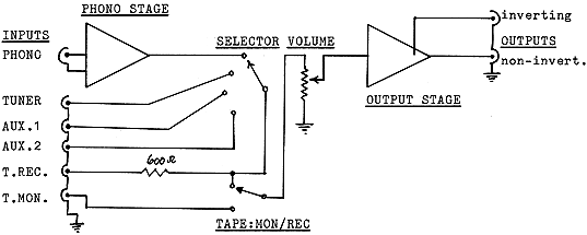
GENERAL CONTROL PREAMPLIFIER LAYOUT
PARTS LIST (for 2 Channels double the amounts in the respective stages) all resistors 1/4W M.F. unless otherwise stated.
PASSIVE RIAA SECTION
R1=93k, R2=7k2, 4.7MegOhms, C2=0.033uF (Polypropylene)
C3=0.01uF/0.001uF/220pF in parallel (Polypropylene/Polystyrene)
0.22uF Mylar/600V
see relevant section for trimming details.
PHONO STAGE
R1=input impedance, values from 5Ohms to 100kOhms must experiment.
C1=minimum 47pF, although can be increased to suit Cartridge.
RL1=10kOhms (x2) RE1=10 Ohms(x2) RI1=100 Ohms
RL2=16kOhms (x2) RE2=130 Ohms (x2) RI2=200 Ohms
R2=10kOhms, R3=6k8 (1/2W), R4=1Meg, C2=4x1.0uF/600V Mylar.
T1=LM394CH, 2N4401 (x2), MPSA05/6 (x2)
T2=2N4092/3, 2N4392/3, 2N5565/6
T3=BC549, LM394ch, 2N4401 etc
T4=2N4401, (or other NPN specified types)
C3=1000uF/16V Electrolytic.
OUTPUT STAGE
V1=10k-100kOhms dual logarithmic taper.
R1=1MegOhms, R2=16kOhms (x2), R3=680 Ohms (x2), R4=10k, R5=200 Ohms
R6=6k8 (x2), R7=1MegOhms (x2), C1=1.0uF/600V Mylar (x2)
T1=2N4092/3, etc (see Phono Stage alternatives)
T2=2N4401 etc (see Phono Stage alternatives)
BUFFER: T1-2N4092, R8=1MegOhms, R0=6k8 Ohms
POWER SUPPLY
R1=1k6 1/2W, R2=R9=R10=R7=100 Ohnms (x7), R3=4k7 Ohms, R4=1.0kOhms
R5=11kOhms, R6=5k6 Ohms, R8=10kOhms
Z1-30V Zener, Z2=20V Zener, T6=2N5459, T1=2N4403 (x3), T5=BC549 (x2)
T2=2N4401, T3=2SA948, BD139, T4=Lm394CH (or 2x2N4401)
C1=4700uF/100V (Electrolytic), C2=1000uF/35V(E), C3=1000uF/25V(E)
C4=2200uF/25V(E)
POWER SUPPLY PARTS
TRANSFORMER: 240/220/120VAC to 50V & 15V Taps
D1-8=1N4004
REGULATOR: 7915 15V negative regulator.
0.1uF/100V Polycarbonate bypass capacitors (x3)
AC Cord, AC Plug.
GENERAL PREAMPLIFIER LAYOUT
Parts required for two PHONO STAGES AND OUTPUT STAGES
SELECTOR SWITCH: 2 pole 4 position Rotary Switch
TAPE SELECTOR
SWITCH: 2 pole 2 position Toggle Switch
RCA or LEMO ("00")
Panel Sockets: 16 of
Ensure that the PHONO and OUTPUTS are insulated from the chassis GND Connetor
2 different Chassis - one for the Primary Filtering and Transformer and the other Housing the Gain Stages and Regulator Circuits.
WIRE: For general wiring of the circuits (special wire for circuitry)
ON/OFF Toggle Switch with indicator light.
TABLE 1. F.E.T. v's BIPOLAR CHARACTERISTICS
In both circuits: RL-16kOhms, RI=200 Ohms
BIPOLAR
| THD | @RMS% | IMD@% | GAIN | NOISE* | |
| RE | 1.0V | 5.0V | 1.0V | dB | dB |
| 0 | 0.05 | 1.10 | 0.13 | 50.5 | 70.5 |
| 10 | 0.04 | 0.99 | 0.10 | 47.5 | 68.0 |
| 39 | 0.02 | 0.40 | 0.05 | 42.0 | 66.5 |
| 130 | 0.01 | 0.17 | 0.04 | 34.0 | 64.0 |
| 680 |
| THD | @RMS% | IMD@% | GAIN | NOISE* | |
| RE | 1.0V | 5.0V | 1.0V | dB | dB |
| 0 | 0.36 | 1.90 | 1.20 | 32.5 | 53.5 |
| 10 | 0.32 | 1.75 | 1.00 | 32.0 | 53.0 |
| 39 | 0.22 | 1.20 | 0.70 | 30.6 | 52.0 |
| 130 | 0.11 | 0.62 | 0.30 | 28.0 | 50.0 |
| 680 | 0.01 | 0.10 | 0.02 | 19.3 | 42.0 |